
Throughout 2025, the Phoenix semiconductor campus demonstrated that advanced chipmaking can thrive on American soil while simultaneously cultivating the workforce, partnerships, and infrastructure necessary for sustained industry leadership.
Manufacturing Achievements Exceed Expectations
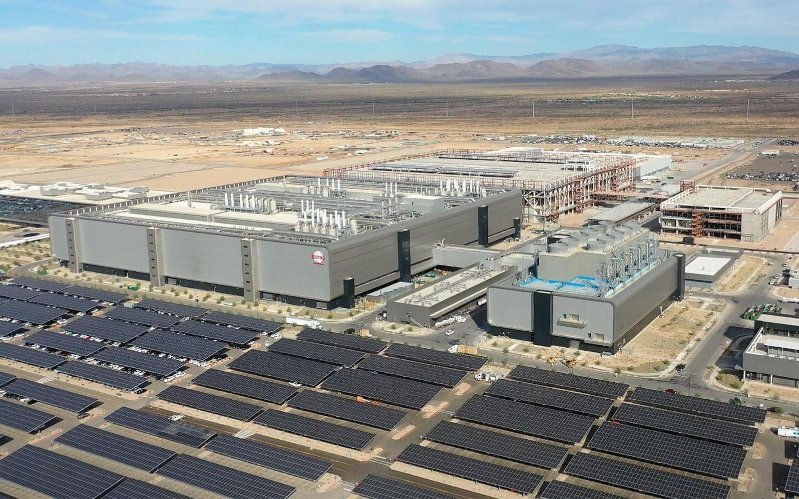
TSMC Arizona’s first fab entered high-volume production at the end of 2024 with a monthly capacity of approximately 30,000 wafers. Customer demand immediately absorbed available capacity, with major technology companies including Apple, AMD, and Nvidia fully booking production slots. Financial results reflected operational maturity, as the Arizona unit generated approximately $150 million USD in net profit during the first half of the year, marking the facility’s transition from startup losses to sustainable profitability.
October witnessed a celebration at the north Phoenix campus when Jensen Huang, Nvidia’s CEO, visited to commemorate the mass production of AI chips manufactured through the partnership between the two companies. Huang emphasized the historic nature of the achievement: “For the very first time in American history, in recent American history, the single most important chip is being manufactured here in the United States by the most advanced fab at TSMC here in the United States.”
The joint venture between TSMC Arizona and Nvidia focuses on producing Blackwell wafers, critical components powering AI data centers worldwide. These large-format wafers represent key technology in the competitive race to enable artificial intelligence applications, with demand continuing to accelerate throughout the year.
Community Investment Through Workforce Development
TSMC Arizona committed $5 million to apprenticeship programs designed to create accessible pathways into semiconductor manufacturing careers. The expanded initiative, announced in collaboration with Governor Katie Hobbs and Phoenix Mayor Kate Gallego, now encompasses four distinct technician specializations supported by partnerships with five educational institutions across the Valley.
Equipment technician apprenticeships operate through Estrella Mountain Community College, while process technician training runs via Northern Arizona University and Rio Salado College. A manufacturing technician specialist intensive program partners with Grand Canyon University and Western Maricopa Education Center, with facilities technician positions continuing at Estrella Mountain.
Rose Castanares, president of TSMC Arizona, characterized the programs as demonstrating “what’s possible when government, industry, and education come together.” She continued: “We are deeply committed to creating job opportunities for local Arizonans. Our newest technician apprentices will get the support and training they need to thrive in their new careers and help us make the most advanced semiconductor technology in the United States.”
The programs combine on-the-job training with classroom instruction over 18 to 24 months, leading to industry-recognized certifications. Participants work full-time while earning their credentials, receiving competitive wages that increase based on time and performance. The company planned to add approximately 130 apprentices during 2025, with applications continuing throughout the year.
Governor Hobbs emphasized the broader implications: “The semiconductor industry has created opportunities for countless Arizonans to gain access to good-paying, stable jobs. Today, we are making that opportunity more accessible by creating new pathways into this growing, high-tech sector through robust new apprenticeship programs.”
Employment projections indicate that once all facilities reach operational capacity, TSMC Arizona will directly employ approximately 12,000 workers. The employment figure represents direct positions across the six planned fabrication facilities and associated infrastructure, not including construction jobs or indirect employment through suppliers and supporting businesses.
Strategic Expansion Responds to Market Demand
March brought the announcement of a $100 billion investment increase, elevating total U.S. commitment to $165 billion. The expansion encompasses three additional fabrication plants, two advanced packaging facilities, and a research and development center. Former Chairman and CEO Dr. C.C. Wei explained the rationale: “AI is reshaping our daily lives, and semiconductor technology is the foundation for new capabilities and applications. With the success of our first fab in Arizona, along with needed government support and strong customer partnerships, we intend to expand our U.S. semiconductor manufacturing investment by an additional $100 billion.”
The announcement positioned the Phoenix campus for evolution into what Former CEO Wei described as a “gigafab cluster” serving customers across smartphones, artificial intelligence, and high-performance computing applications. The company indicated it was close to securing additional land parcels adjacent to current facilities to accommodate the expanded footprint.
Technology deployment accelerated in response to customer requirements. During July earnings discussions, Wei revealed plans to “upgrade our technologies faster to N2, and more advanced technology to Arizona,” citing strong interest from leading U.S. customers. The second fab, which completed the shell of construction during 2025, will manufacture 3-nanometer chips before
The third fab, which broke ground in April with Commerce Secretary Howard Lutnick attending, now projects production commencement by the end of the decade. This facility will host 2-nanometer and angstrom-class A16 processes, representing the company’s most advanced manufacturing capabilities.
Nvidia emphasized the strategic importance of domestic production capacity. A company spokesperson stated: “AI is revolutionizing every aspect of the technology stack, and Nvidia AI supercomputers are at the foundation. We’re proud to produce our technology in Arizona, bringing AI infrastructure manufacturing back to America. The administration’s support for U.S. manufacturing makes this possible—and vital—for the next industrial revolution.”
Educational Partnerships Strengthen Innovation Ecosystem
The ASU-TSMC partnership operates across multiple dimensions. Master’s fellowships and scholarships support thesis-track students aligned with semiconductor research. Laboratory course support doubled the number of students participating in hands-on learning related to semiconductor manufacturing. Faculty engagement includes research support through mentorship programs and joint workshops advancing semiconductor technology.
The Corporate Affiliate Program provides structured pathways for ASU students entering TSMC Arizona operations, initially targeting juniors, seniors, and graduate students for engineering, manufacturing, business, and infrastructure internships. Connection with ASU’s Access ASU program introduces semiconductor career paths to high school and transfer students, expanding the entry points into the industry.
Economic Impact Radiates Across Region
Chris Camacho, president and CEO of the Greater Phoenix Economic Council, quantified the ecosystem effect: since TSMC’s initial commitment, GPEC has located 39 semiconductor-related companies to the region, creating more than 7,700 jobs and over $37 billion in capital investment. Fourteen of TSMC’s key suppliers established or announced U.S. facilities to support Arizona operations, creating clustering effects that multiply economic benefits.
The Greater Phoenix area now hosts more than 75 semiconductor companies. This concentration prompted the Semicon West conference to relocate from San Francisco to Phoenix starting in 2025, ending a 50-year run in the Bay Area. The shift signals industry recognition of Arizona’s emergence as a genuine semiconductor hub rather than a satellite operation.
Economic projections for TSMC Arizona’s investment indicate the generation of approximately $1.2 billion in direct tax revenues plus $195 million in indirect tax revenues over a 13-year period. Personal income creation is estimated at $4.6 billion direct plus $4.8 billion indirect for a total of $9.3 billion, while economic output should reach $32.9 billion.
Phoenix Mayor Kate Gallego characterized the transformation: “As we continue to grow our semiconductor industry in Phoenix and the region, this new partnership between ASU and TSMC will create a strong talent pipeline for years to come, filling new, good-paying jobs and ultimately boosting our local economy.”
Technical Leadership Drives Competitive Position
The Phoenix facility’s production of 4-nanometer chips using the N4 process node places it at the forefront of commercial semiconductor manufacturing. The second fab’s planned 3-nanometer and 2-nanometer capabilities will maintain technological parity with the most advanced facilities globally. TSMC Arizona is committed to deploying its A16 process, representing technology beyond traditional 2-nanometer classifications, at the Phoenix campus rather than reserving cutting-edge processes exclusively for Taiwan operations.
Former CEO Wei confirmed confidence in quality consistency: “We are confident to deliver the same level of manufacturing quality and reliability from our fab in Arizona as from our fabs in Taiwan.” The yield performance data validated this assertion, demonstrating that advanced chipmaking can achieve world-class results in U.S. facilities when supported by appropriate investment, workforce development, and operational expertise.
Each of the three fabs under construction features cleanroom areas approximately double the standard industry logic fab size, accommodating extensive equipment requirements for leading-edge production. The facilities incorporate TSMC’s global standards for green manufacturing, including targets for 90% water recycling rates through planned industrial water reclamation infrastructure.
The concentration of advanced manufacturing capacity, research facilities, workforce training programs, and supplier networks positions Arizona as a critical node in global technology supply chains. The transformation reduces dependence on overseas production for chips essential to national security and economic competitiveness while demonstrating the viability of domestic advanced semiconductor manufacturing when industry, government, and academia align toward shared objectives.
For the semiconductor industry and the communities hosting these operations, 2025 established that technical excellence, economic opportunity, and strategic resilience can advance simultaneously through sustained commitment to manufacturing innovation and workforce investment.