
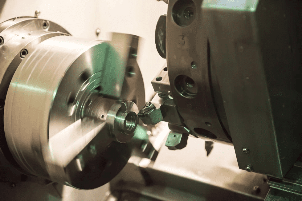
The semiconductor industry operates on a level of precision that borders on invisible. Every microchip, sensor, and wafer relies on components manufactured with microscopic accuracy. A single defect can compromise an entire production line. These factors make precision machining and manufacturing essential.
Let’s explore how precision machining achieves the ultra-tight tolerances that define the future of technology.
Why Ultra-Tight Tolerances Are Non-Negotiable
In semiconductor fabrication, even the smallest imperfection can lead to massive losses. The scale is precise: tolerances are often measured in micrometers (μm), and in some instances, even nanometers. Every part must perform flawlessly under extreme conditions.
- Wafer Integrity: Components such as chucks, vacuum chambers, and wafer carriers must maintain perfect flatness and dimensional stability. Even microscopic unevenness can scratch or warp wafers, resulting in costly rework or scrapped batches.
- Equipment Performance: Lithography and deposition tools rely on exact alignment. A deviation of only a few micrometers can shift patterns and ruin hundreds of chips, costing manufacturers millions in lost production.
- Vacuum and Purity: The semiconductor process demands absolute cleanliness. Machined parts used in vacuum environments must have ultra-smooth surfaces and tight seals to prevent leaks or contamination that could destroy delicate layers of material.
These requirements make precision machining and manufacturing an essential foundation of semiconductor fabrication.
How Precision Machining Achieves Micrometer-Level Accuracy
Achieving this microscopic accuracy is no coincidence. It depends on a combination of advanced technology, specialized expertise, and environmental control.
1. Multi-axis CNC machining.
Modern CNC machines with 5-axis capability can produce complex geometries in a single setup. This eliminates the risk of tolerance stacking that occurs when parts are repositioned multiple times.
2. Advanced stable materials.
Semiconductor equipment often uses high-purity aluminum, stainless steel, ceramics, quartz, single-crystal silicon, and specialty alloys like Invar, because they maintain stability under heat and vacuum. Many components also rely on specialized expertise, such as titanium CNC machining services, as titanium provides superior strength-to-weight ratios and resistance to corrosion in high-vacuum environments.
3. Controlled manufacturing environment.
Even small temperature fluctuations can cause metal to expand or contract. Precision machining facilities use temperature-controlled rooms to maintain consistency down to the micrometer.
4. State-of-the-art metrology.
Quality verification is as critical as machining itself. Coordinate measuring machines (CMMs), laser interferometers, and optical profilometers measure components against exacting specifications, ensuring that every surface, bore, and edge meets tolerance before assembly.
Together, these factors enable manufacturers to meet the semiconductor industry’s exacting standards and push the limits of modern technology.
Precision Engineering Machining Services as a Key to Semiconductor Progress
Precision machining is far more than a manufacturing process: it’s an enabler of progress. Through expert control of materials, machines, and measurement, precision engineering machining services ensure that semiconductor equipment performs with unmatched reliability. The result is higher yields, fewer defects, and faster innovation cycles across the industry.
For manufacturers seeking consistency and scalability, partnering with specialists in precision machining and manufacturing is an investment in performance and peace of mind. Schedule a consultation to learn how advanced titanium CNC machining services and other precision capabilities can help your operations achieve semiconductor-grade accuracy and efficiency.