
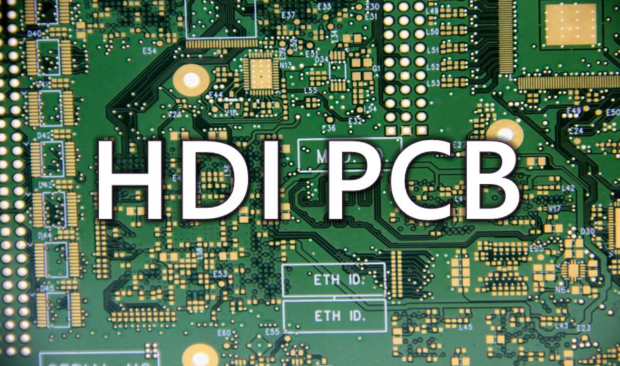
Modern electronic products continue to shrink in size while integrating more functionality, higher processing power, and faster communication. Smartphones, wearable devices, medical instruments, automotive control units, and networking equipment all require increasingly complex printed circuit boards within limited space. Achieving these design goals depends not only on HDI technology itself but also on selecting an experienced hdi pcb manufacturer capable of producing high-density designs with consistent process control and tight manufacturing tolerances.
As component pitch decreases and routing density increases, manufacturing quality has a direct influence on electrical performance, assembly yield, and long-term reliability. Features such as laser-drilled microvias, controlled impedance, precise layer registration, and accurate via filling require specialized equipment and validated manufacturing processes that extend beyond conventional PCB fabrication.
What Is an HDI PCB?
A High-Density Interconnect (HDI) PCB is designed to accommodate more electrical connections within a smaller board area by using advanced fabrication techniques and tighter design rules than standard multilayer PCBs.
Common HDI technologies include:
- Laser-drilled microvias
- Blind and buried vias
- Sequential lamination
- Via-in-pad structures
- Copper-filled microvias
- Fine-line imaging
- High-density routing
- Controlled-impedance manufacturing
Rather than simply adding more layers, HDI manufacturing allows designers to optimize routing between fine-pitch components such as BGAs, processors, memory devices, and RF modules while making efficient use of available board space.
How HDI Manufacturing Supports Miniaturization
Miniaturization depends as much on manufacturing capability as circuit design. While HDI layouts allow higher component density, the fabrication process determines whether those designs can be produced consistently.
Laser-drilled microvias occupy far less area than mechanically drilled through-holes, creating additional routing channels beneath high-pin-count components. Blind and buried vias further reduce congestion by connecting only the required layers instead of passing through the entire board.
Sequential lamination enables multiple HDI build-up layers, allowing complex interconnections without excessive board thickness. Via-in-pad technology permits direct placement of components over vias, making efficient use of valuable PCB real estate when properly filled and planarized.
Fine-line imaging supports narrower traces and reduced spacing, enabling designers to route more signals within constrained layouts while meeting manufacturing tolerances.
Together, these manufacturing processes allow engineers to develop thinner and more compact electronic assemblies without relying solely on larger multilayer boards.
Manufacturing Practices That Influence Signal Performance
Higher operating frequencies and increasing data rates place greater demands on PCB manufacturing accuracy. HDI technology can support signal integrity objectives, but electrical performance depends on the complete design and fabrication process rather than HDI construction alone.
Manufacturing factors that contribute to consistent electrical performance include:
- Accurate controlled-impedance manufacturing
- Precise layer registration
- Uniform copper thickness
- Stable dielectric materials
- Consistent microvia geometry
- Well-controlled trace width and spacing
Shorter routing paths and optimized via structures may help reduce discontinuities in high-speed circuits. However, improvements in signal loss, electromagnetic interference (EMI), and overall performance depend on stack-up design, material selection, PCB layout, via structure, and manufacturing tolerances working together.
Because of these interactions, HDI fabrication typically involves close collaboration between PCB designers and manufacturing engineers during design-for-manufacturability (DFM) review.
Critical Manufacturing Processes Behind Reliable HDI Boards
Producing reliable HDI PCBs requires precise control over several specialized fabrication processes.
Laser Microvia Formation
Laser drilling creates small-diameter microvias with accurate positioning for high-density interconnections. Consistent drilling parameters help maintain uniform via dimensions throughout production.
Copper Plating and Via Filling
Microvias require sufficient copper plating to withstand thermal cycling during assembly and field operation. Copper-filled vias are commonly used for via-in-pad designs, providing a flat surface for component placement while supporting solder joint quality.
Sequential Lamination
Each lamination cycle must maintain accurate alignment between newly added layers and existing circuitry. Process control becomes increasingly important as layer count and routing density increase.
Fine-Line Imaging
High-resolution imaging systems define narrow traces and spacing that support dense routing beneath fine-pitch components. Registration accuracy directly affects manufacturing yield and conductor integrity.
Controlled-Impedance Manufacturing
Many HDI products incorporate high-speed digital or RF interfaces requiring controlled impedance. Manufacturers verify trace geometry, dielectric thickness, and copper characteristics to achieve specified impedance targets within acceptable tolerances.
Reliability Risks in HDI PCB Manufacturing
Advanced HDI designs introduce manufacturing challenges that require careful process control and inspection.
Insufficient Microvia Plating
If copper plating inside microvias is too thin or inconsistent, thermal expansion during soldering and operation may increase the likelihood of fatigue-related failures over time.
Stacked Microvia Cracking
Stacked microvias concentrate mechanical and thermal stresses at specific locations. Poor process control or unsuitable design choices can increase the risk of cracking during repeated thermal cycles.
Layer Misregistration
Misalignment between layers can affect annular rings, routing accuracy, impedance consistency, and overall manufacturability. Precise optical alignment and registration verification help minimize these issues.
Poor Via-Fill Planarity
Incomplete or uneven copper filling may create surface irregularities that interfere with component placement, solder paste deposition, and assembly quality, particularly for fine-pitch BGAs using via-in-pad construction.
Manufacturers typically address these risks through process monitoring, inspection, cross-section analysis, plating verification, and electrical testing rather than relying on design features alone.
Design for Manufacturability Matters
Even well-designed HDI layouts benefit from early manufacturing review.
DFM analysis helps identify features that may reduce fabrication yield or increase production risk before manufacturing begins. Typical review items include:
- Trace width and spacing
- Microvia aspect ratios
- Via stacking strategy
- Copper balancing
- Annular ring dimensions
- Layer transitions
- Component spacing
- Controlled-impedance requirements
Resolving manufacturability concerns during the design stage often reduces engineering revisions and improves production consistency.
Applications Requiring High-Density Manufacturing
HDI manufacturing supports products that combine compact form factors with demanding electrical performance requirements. Common examples include consumer electronics, networking hardware, medical devices, industrial control systems, telecommunications equipment, automotive electronics, aerospace assemblies, and embedded computing platforms.
Across these applications, the primary advantage lies not in a specific industry but in the ability to fabricate dense interconnect structures while maintaining manufacturing consistency for complex multilayer designs.
How to Evaluate an HDI PCB Manufacturer
Selecting an HDI PCB manufacturer involves more than confirming support for microvias or multilayer construction. Manufacturing capability should align with the technical requirements of the intended design.
Areas to evaluate include:
- Experience with laser-drilled microvias, blind and buried vias, and sequential lamination
- Proven capability for copper via filling and via-in-pad fabrication
- DFM support during early design stages
- Controlled-impedance manufacturing and verification
- Layer registration accuracy for complex multilayer boards
- Electrical testing, cross-section analysis, and inspection procedures
- Process controls for plating consistency and dimensional accuracy
Reviewing these capabilities helps determine whether a manufacturer can consistently produce complex HDI designs while supporting quality objectives throughout production.
Conclusion
HDI technology enables increasingly compact and capable electronic products, but successful implementation depends on manufacturing expertise as much as PCB design. Processes such as laser microvia drilling, sequential lamination, fine-line imaging, controlled-impedance manufacturing, accurate layer registration, and reliable copper via filling all contribute to producing dense interconnect structures that can be manufactured consistently.
Equally important is understanding the manufacturing risks associated with advanced HDI fabrication, including microvia plating quality, stacked-microvia reliability, registration accuracy, and via-fill planarity. Addressing these considerations through DFM review, process control, inspection, and verification helps improve production outcomes for demanding electronic designs.
To learn more about HDI PCB fabrication, rapid prototyping, and advanced manufacturing capabilities, visit Fast Turn PCB.