
Introduction
The evolution of transistors is one of the most fascinating stories in the history of modern technology. From their invention in the late 1940s to today’s nanoscale microchips powering artificial intelligence and smartphones, transistors have revolutionized electronics and computing. The journey from bulky vacuum tubes to billions of tiny transistors packed into a single chip highlights the extraordinary progress in the history of semiconductor technology.
In the early days of computing, machines relied on vacuum tubes that were large, fragile, and consumed enormous amounts of electricity. These limitations slowed technological progress. However, the breakthrough invention of the transistor at Bell Labs completely transformed the electronics industry. Over time, continuous innovation in semiconductor miniaturization, wafer fabrication, and advanced lithography enabled transistors to become smaller, faster, and more energy efficient.
Today, the evolution of transistors has reached astonishing levels, where billions of microscopic switches operate within modern microchips. This progress directly influenced computing advancements discussed in transistor history, the development of processors, and the rise of history of computer processors.
Understanding the evolution of transistors helps explain how the digital world—from smartphones to supercomputers—became possible.
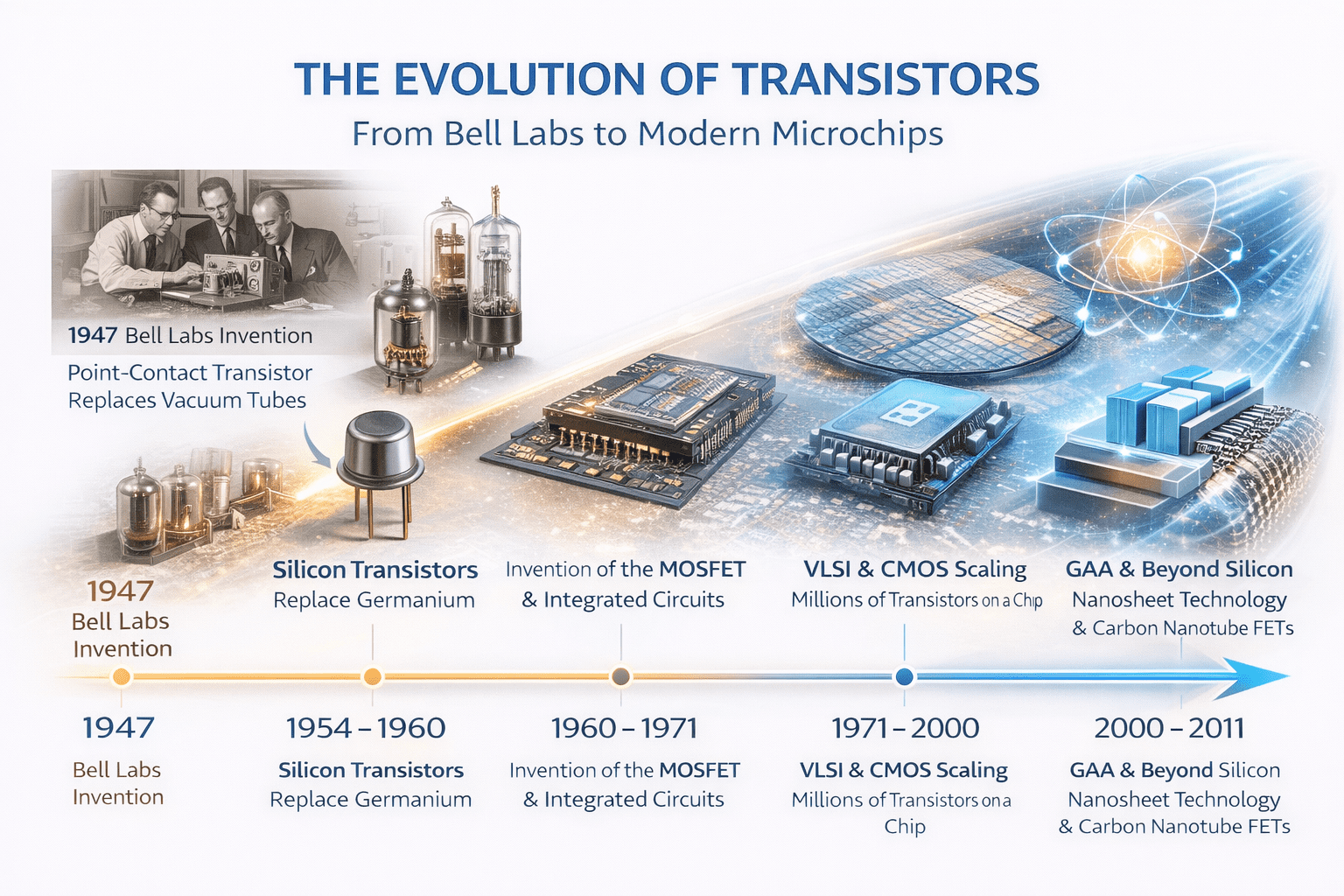
A. 1947 – 1954: The Breakthrough at Bell Labs
The first major milestone in the evolution of transistors occurred in 1947 at Bell Labs, where scientists successfully created the first working transistor.
Shockley, Bardeen, and Brattain: The Point-Contact Discovery
John Bardeen, Walter Brattain, and William Shockley developed the first transistor using P-type and N-type semiconductors. Known as the point-contact transistor, it controlled electron flow through semiconductor materials.
This discovery was revolutionary because it replaced unreliable vacuum tubes with a much smaller and more efficient component. The transistor was based on semiconductor physics and the behavior of electrons within doped materials called dopants.
The invention marked the beginning of the evolution of transistors, launching a new era in electronics.
Replacing the Vacuum Tube: The Efficiency Revolution
Before the transistor, computers relied on vacuum tubes, which generated excessive heat and frequently failed. Early computers like ENIAC used thousands of tubes that required constant maintenance.
The transistor solved these issues by providing a smaller, cooler, and more reliable alternative. This dramatic shift represented the first step in the evolution of transistors, enabling more compact electronic devices.
B. 1954 – 1960: The Shift from Germanium to Silicon
As research continued, engineers improved transistor materials to enhance performance and reliability.
Texas Instruments and the First Commercial Silicon Transistor
In 1954, Texas Instruments produced the first commercial silicon transistor. Silicon proved to be far more stable than germanium at higher temperatures.
This innovation accelerated the evolution of transistors, allowing manufacturers to create more reliable electronic components for radios, military systems, and early computing devices.
Why Silicon Became the Industry Standard
Silicon eventually became the dominant material for semiconductor manufacturing due to its excellent electrical properties and abundance in nature.
Silicon wafers allowed engineers to perform precise wafer fabrication processes and introduce dopants to control electron flow efficiently. These advances significantly influenced the evolution of microchips and enabled the next generation of integrated circuits.
C. 1960 – 1971: The Invention of the MOSFET and Integrated Circuits
The next critical stage in the evolution of transistors occurred when scientists invented a new type of transistor called the MOSFET.
Mohamed Atalla and the Metal-Oxide-Semiconductor Field-Effect Transistor
Mohamed Atalla developed the MOSFET, which uses a metal-oxide layer to control electrical current through a semiconductor channel.
This transistor design enabled higher efficiency and easier miniaturization compared to earlier Bipolar Junction Transistor (BJT) designs. The MOSFET quickly became the foundation of modern integrated circuits.
Because MOSFETs could be scaled down easily, they played a major role in the transistor scaling journey that followed.
The Birth of the Microprocessor: Putting it All on One Chip
In 1971, Intel introduced the first commercial microprocessor, integrating thousands of transistors onto a single silicon chip.
This development marked a turning point in the evolution of transistors, because it allowed entire computing systems to fit onto small chips.
The integration of multiple circuits onto one chip triggered rapid innovation in semiconductor miniaturization and set the stage for the digital revolution.
D. 1971 – 2000: Scaling and the Evolution of Transistors Milestone
Between the 1970s and 2000, the evolution of transistors accelerated rapidly as engineers improved chip manufacturing processes.
CMOS Technology: Solving the Heat and Power Crisis
Complementary Metal-Oxide-Semiconductor (CMOS) technology dramatically improved energy efficiency by using both P-type and N-type transistors.
CMOS circuits consumed far less power than earlier designs and reduced heat generation. As a result, CMOS became the dominant architecture for microchips and modern processors.
This advancement was essential in overcoming Moore’s Law limits and enabling faster computing systems.
VLSI (Very Large Scale Integration): Millions of Gates on a Die
VLSI technology allowed engineers to place millions of transistors onto a single chip using advanced lithography (nm) techniques.
The introduction of VLSI marked a massive leap in the evolution of transistors, enabling complex processors, graphics chips, and memory devices.
This period also laid the groundwork for modern computing innovations and the emergence of modern artificial intelligence applications that rely on powerful microchips.
E. 2000 – 2011: Overcoming Quantum Leakage with 3D Architectures
By the early 2000s, semiconductor engineers encountered serious challenges related to transistor scaling.
High-K Dielectrics: Reinventing the Gate Insulator
As transistors shrank to nanometer sizes, quantum tunneling began causing leakage currents that reduced efficiency.
To solve this problem, researchers introduced high-k dielectric materials that improved transistor performance while minimizing power loss.
These innovations allowed the evolution of transistors to continue despite growing physical limitations.
The FinFET Revolution: Moving from 2D to 3D Transistors
The FinFET architecture represented a major breakthrough in semiconductor engineering.
Unlike traditional flat transistors, FinFET designs use a 3D fin structure to control electron flow more effectively. This improvement reduced leakage and increased performance.
FinFET technology enabled chip manufacturers to maintain the momentum of the evolution of transistors while pushing transistor sizes below 20 nanometers.
F. 2011 – 2026: The Future of Nanosheets and Atomic Logic
Today, semiconductor research continues to push the boundaries of physics.
Gate-All-Around (GAA) Transistors: Scaling Below 3nm
Gate-All-Around (GAA) transistors represent the next stage in the evolution of transistors.
In this design, the gate completely surrounds the channel, providing precise control over electron movement. This structure allows engineers to continue scaling transistors below 3 nanometers.
GAA technology represents one of the most promising solutions to Moore’s Law limits.
Beyond Silicon: Exploring Graphene and Carbon Nanotube FETs
Researchers are also investigating alternative materials such as graphene and carbon nanotubes to replace traditional silicon transistors.
These materials offer superior electrical conductivity and could enable the next generation of ultra-fast microchips.
If successful, these innovations will define the future of the evolution of transistors and transform the computing landscape.
Frequently Asked Questions (FAQs)
What is the evolution of transistors?
The evolution of transistors refers to the technological progress from early point-contact transistors to modern nanoscale semiconductor devices used in microchips.
Why did transistors replace vacuum tubes?
Transistors replaced vacuum tubes because they are smaller, more reliable, energy-efficient, and generate less heat.
What role do MOSFETs play in modern electronics?
MOSFETs are the most widely used transistors in modern electronics and form the foundation of integrated circuits and microprocessors.
What challenges affect transistor scaling today?
Modern challenges include quantum tunneling, heat dissipation, and the physical limits of silicon materials.
Conclusion
The evolution of transistors represents one of the most important technological journeys in modern history. From the first point-contact transistor invented at Bell Labs to today’s nanoscale devices powering advanced computing systems, transistors have transformed electronics and computing.
Continuous innovation in semiconductor miniaturization, materials science, and microchip design has enabled the development of powerful processors, smartphones, and artificial intelligence systems.
As engineers explore new materials like graphene and carbon nanotubes, the evolution of transistors will continue to shape the future of technology for decades to come.